If you’ve been following the development of additive manufacturing (AM) systems focused on the electronics industry, you’ve heard about Nano Dimension. In 2012, the company began developing its dual-material DragonFly system for 3D-printing prototype multi-layer printed circuit boards (PCBs). The approach combines inkjet technology with 3D printing using proprietary nanotechnology-based conductive and dielectric inks. Users are able to produce their own complex, high quality prototype PCBs in hours instead of days or weeks (the usual turn-around time for out-sourced boards).
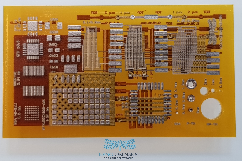 3D-printed multilayer PCB. Top layer displays traces with various trace- and space-widths, as well as non-plated and plated through-holes and vias. Produced on the DragonFly 2020 Pro 3D Printer from Nano Dimension. (Image courtesy Nano Dimension)
Nano Dimension has used feedback from beta testing its first-generation systems to develop and announce, on September 13, a larger, commercial model called the DragonFly 2020 Pro 3D Printer. This version has been optimized to quickly move electronics hardware development from proof of concept through design validation to test-fixture creation, in formats and materials of true PCBs. The result: faster revisions and more creative board layouts, speeding up board-design approval for downstream manufacturing.
PCBs in Hand, in House
“Optimizing workflows shrinks PCB design and test cycles from months or weeks, to days,” says Simon Fried, co-founder and CBO of Nano Dimension. “More and easier iterations lead to greater innovation and better business outcomes.” Traditionally, PCB designers send their Gerber (standard PCB layout) files to an outside vendor for production, even for a single board. If users can print and test a board within hours of its design, they will be able to prove functionality and try out more variations, all with shorter turnarounds.
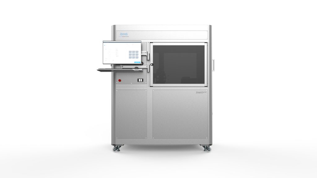 The DragonFly 2020 Pro 3D printer from Nano Dimension is now ready for commercial use. Its dual material system lets users 3D-print prototype multi-layer printed circuit boards (PCBs), saving time and supporting more design explorations. (Image courtesy Nano Dimension)
The DragonFly 2020 Pro offers a build volume of 20 x 20 x 0.3cm (approximately 8 x 8 x 0.12 inches), inside a unit that sits on the floor and measures 140 x 80 x 180cm. Currently, the company is putting all its efforts into this Pro version, though the plan is to offer additional models in the future.
General printing capabilities are: 100 micron traces, 125 micron spaces, and a minimum layer thickness of 3 microns, with the number of layers only limited by the Z axis.
Print speed depends, of course, on the number of layers, board size and overall circuit complexity. However, Nano Dimension notes, in general, a complex 10-layer board could be printed overnight.
Growing the 3D-Printing Business
Beta customers of the first DragonFly system included companies involved in defense work, solar energy and PCB design, demonstrating the wide range of end applications. The results of that test program provided feedback for fine-tuning the next generation Dragonfly 2020 Pro system, and user interest is growing.
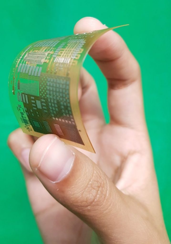 3D-printed PCB produced on the DragonFly 2020 Pro by Nano Dimension opens up possibilities for flexible electronics applications. (Image courtesy Nano Dimension)
Last month Nano Dimension announced that Jabil has signed an agreement as its first commercial customer. Jabil is a manufacturing solutions company providing comprehensive design, production and product management services to global electronics and technology companies. The DragonFly 2020 Pro is expected to be delivered in mid-November and will be evaluated at the Jabil St. Petersburg, FL, Design Center. The Design Center focuses on quick-turn prototyping PCB board designs to reduce the time to evaluate new solutions while speeding time-to-market.
Also in 2017, Nano Dimension received funding for two new collaborative projects developing 3D-printed parts for space applications. With Harris Corporation, the program will develop 3D-printed electronic modules for space applications; the goal is to combine digital, RF signal and power functions on a double-sided, multi-layer board without requiring manual assembly.
With Semplastics, a company that produces both precision plastic components and high-performance materials, Nano Dimension will demonstrate its versatility in materials development. The two companies will build complex ceramic test objects using Semplastics-developed ceramic materials blended into modified Nano Dimension 3D-printing resins. The goal is to rapidly and inexpensively produce lightweight objects featuring complex designs yet demonstrating high mechanical stability.
Buy or Lease a DragonFly 2020 Pro 3D Printer
Nano Dimension is growing its distribution network worldwide, having recently announced partnerships with Anglo Production Processes (UK and Ireland), CADvision (France, Belgium, Switzerland), Cadlog (Italy), Emona Instruments (Australia), and CAD MicroSolutions (Canada).
Prospective customers can now get quotes to buy or lease the DragonFly 2020 Pro through Nano Dimension’s Early Access Program.
About the Author
Follow Robotics 24/7 on Linkedin
Article topics
Email Sign Up

Related Manufacturing News