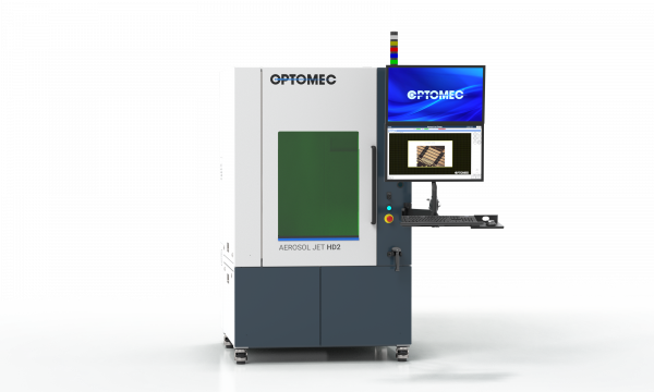
Optomec is announcing an advanced electronics packaging solution for miniaturization of mobile and wearable products. The Aerosol Jet HD2, uses Optomec’s Aerosol Jet 3D Electronics Printing solution to produce high-resolution circuitry, including an ability to dispense conformal 3D interconnects between die, chips, components and substrates. This interconnect approach offers improved performance at high frequencies, especially for 5G and mmWave applications.
Optomec’s Aerosol Jet HD2 targets the existing $4 Billion market for back-end semiconductor packaging and assembly equipment. The Aerosol Jet solution works by precision jetting or “printing” an extremely fine mist of nanoparticle-based inks onto a surface.
The HD2 can print features as narrow as 10 microns with placement accuracy under 5 microns. The nanoparticles are then sintered together, forming a solid metal conductor of copper, gold or silver. Insulating and adhesive materials can also be applied by the Aerosol Jet process with various integrated circuit packaging dielectric materials.
As a primary application, the Aerosol Jet HD2 can serve as a drop-in replacement for the method of connecting electrical components with wire bonds, which have some deficiencies. First, wire bonds require high impact mechanical contact with the IC, often producing scrap, especially with fragile, next-generation gallium-based chips. Second, wire bond loops require extra space within the package, making it harder for designers to create sleek, miniature devices to meet the demands of consumer electronics. Third, wire bonds can choke off the high-frequency mmWave signals required for 5G communications, automotive radar and many other emerging applications.
“The HD2 really changes the way designers think about IC packaging,” says Bryan Germann, aerosol jet product manager. “Not only can it reduce the size of the final electronics package, but it also out-performs wire bonding when it comes to high-frequency signals. Wire bonds simply produce a lot of inductance for RF applications above 40 GHz.”
The HD2 electronics printer also can be used to print transmission lines, sensors and antennas on various materials including common polymers, IC materials, FR4, glass, ceramic and metals. The HD2 was designed for high volume manufacturing and includes production-friendly software that guides operators through a simplified start-up process, ensuring QA compliance. The machine is also available with an in-line conveying option for automated part loading. It can process substrates or part trays up to 300-mm wide and is available with a rotate table for four-axis processing.
About the Author
Press releases may be sent to them via [email protected]. Follow Robotics 24/7 on Facebook
Follow Robotics 24/7 on Linkedin
Article topics
Email Sign Up

Related Optomec News