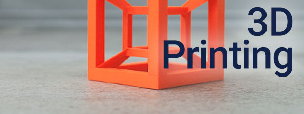
The oft-voiced complaint by those who regard additive manufacturing (AM) as nothing more than a rapid prototyping tool is that the technology is able to compete with existing manufacturing methods when it comes to mass production. While that may be true in some cases (for now), limiting your view of what is possible based on one type of production is a losing game.
Although a press might be able to pump out more parts in a shorter time than an AM system, someone still has to assemble those parts. Time saved in production may well be lost in assembly. Printed during a single build, in situ, embedded electronics are an example of how AM can compete with and complement existing manufacturing methods, and Optomec has announced a breakthrough in that field.
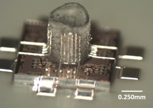 An example of a completed, fully printed dipole antenna microstructure. Courtesy of Optomec.
According to the company, Optomec has developed an improved method of printing at the micron scale using its aerosol jet technology, which allows for printing 3D polymer and composite structures with embedded electronics. Even better, the process works without the need for support structures.
“This breakthrough in 3D printing technology extends additive manufacturing to the creation of micron scale, free-form polymer structures and smart devices,” said Mike O’Reilly, Optomec director of aerosol jet product management. “Early adopter customers have already developed innovative applications for smart devices and micro-fluidic applications. We continue to place emphasis on innovation such as Aerosol Jet 3D micro-structure printing to address our customer’s next generation product development challenges.”
The new process is enabled by a combination of Optomec’s aerosol jet printing, and a proprietary in-situ curing method that enables real-time solidification options. Structures built using the new process can be metalized with conductive traces and may include functional components, such as antennas or sensors. The end result is a fully functional, embedded electronic component.
Optomec claims the process is capable of building structures with lateral feature sizes down to 10 microns, and lateral and vertical build resolutions from 1 micron to 100 nanometers, respectively. Below you’ll find a video from Optomec which demonstrates printed electronics.
Source: Optomec
About the Author
Follow Robotics 24/7 on Linkedin
Article topics
Email Sign Up


Related Manufacturing News